TRANSMISSION // 2611.12850v1
Stressed thin films could make silicon qubits’ valley splitting more predictable
Source published
Simulations suggest that patterned titanium nitride films above silicon quantum-dot gates can generate strain strong enough to enhance valley splitting. The proposed architecture could serve narrow dot arrays, but fabrication, electrical noise and qubit performance remain experimental questions.
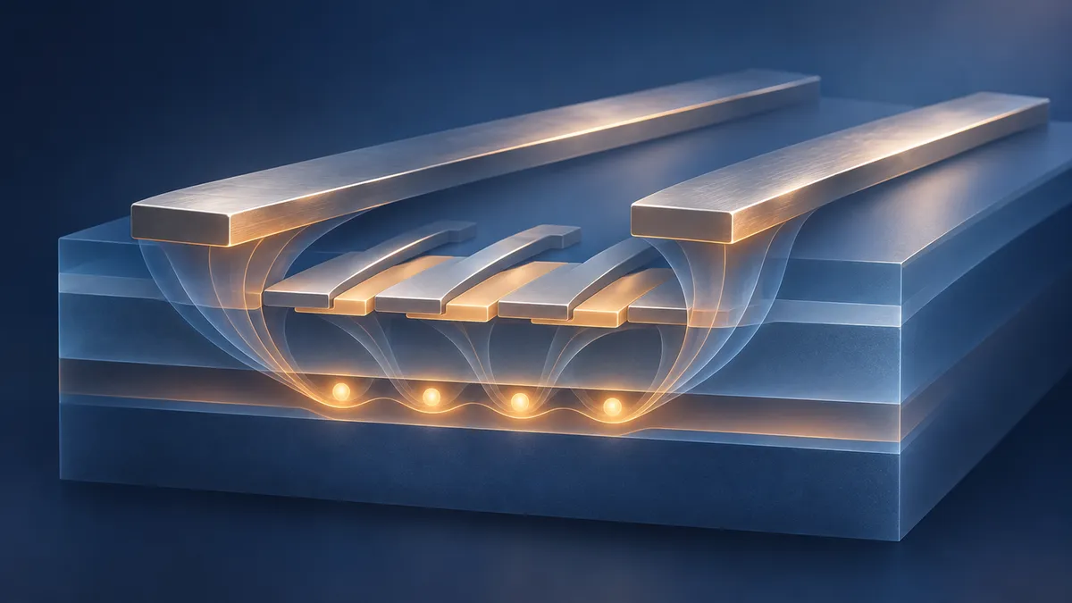
Silicon spin qubits face an atomic-scale consistency problem: an important energy gap can vary unpredictably between quantum dots. A new preprint proposes using deliberately stressed surface films to add a more predictable contribution to that gap, without removing large sections of the underlying semiconductor.
Why the energy gap matters
In silicon quantum dots, electrons have closely spaced states associated with features of the crystal’s electronic structure called valleys. The energy separation between the lowest valley states—valley splitting—is important for silicon spin-qubit operation. Small and inconsistent splittings are an obstacle to scaling these devices.
In silicon/silicon–germanium structures, random arrangements of atoms can make valley splitting vary substantially from dot to dot. Increasing germanium content can raise the average splitting, but does not eliminate locations with very small gaps. The goal is therefore an engineered contribution that depends less on atomic chance.
The proposed solution combines two ingredients: a quantum well with an oscillating germanium concentration, known as a Wiggle Well, and shear strain that changes the crystal’s symmetry. This study investigates how to supply that strain above realistic control gates.
A patterned film supplies the strain
Long-period Wiggle Wells have already been grown in earlier experiments. Their germanium concentration oscillates over distances around 1.7–1.8 nanometres. But crystal symmetry suppresses the valley coupling these oscillations could otherwise produce. Previous theory predicts that adding shear strain can enable that coupling and create a deterministic contribution to valley splitting.
The new proposal uses patterned titanium nitride films carrying residual compressive stress. When bonded to the device surface, these films deform the semiconductor beneath them. Their shape and alignment determine whether that deformation produces the useful shear component relative to the silicon crystal axes.
Geometry matters: a square stressor produces no such shear directly beneath its centre in the symmetric model. Elongated rectangles break that symmetry. The researchers found that the central response approached saturation at a length-to-width ratio of roughly four to one.
Pairs of stressors offer another advantage. Their edge-generated strain fields can reinforce one another in the gap between them, where quantum dots could sit.
What the simulations tested
The researchers used finite-element calculations in COMSOL, progressing from single stressors to paired films, simplified aluminum gates and a realistic four-dot gate layout. The models included silicon’s direction-dependent elastic properties, stress already present in deposited films and thermal contraction.
A representative semiconductor stack contained a 9-nanometre silicon well beneath a 30-nanometre silicon–germanium spacer and a 10-nanometre insulating layer. Strain was evaluated near the top of the well, where the low-energy electron wave functions are concentrated.
In one simplified paired-stressor geometry, separations of approximately 150–350 nanometres produced the largest central shear strain. That range is specific to the modeled dimensions, not a universal optimum.
The realistic gate-stack calculations used 200-nanometre-thick titanium nitride stressors with a compressive residual stress of 3.8 gigapascals, adopting film parameters reported in earlier literature.
Encouraging strain, not a demonstrated qubit improvement
The calculations predict shear-strain magnitudes exceeding 0.1% despite the intervening gates. Combined with earlier strain-assisted Wiggle Well theory, such strains imply deterministic valley-splitting contributions above 100 microelectronvolts, with representative predictions reaching hundreds of microelectronvolts. These are predictions, not measured gaps in newly fabricated devices.
Gates weaken strain transfer partly by lifting the stressors farther from the quantum well. Thicker films can compensate, although the gains diminish with increasing thickness.
The strongest strain occurs near particular stressor edges. A different orientation sacrifices some peak strength but produces a relatively large, uniform strain along the modeled dot channel—potentially useful for extending a linear array.
What still needs testing
The useful region is narrow. The studied layouts naturally suit linear arrays or arrays only a few rows wide; substantially wider two-dimensional devices would need additional stressors or redesigned geometries.
Fabrication also couples variables that simulations can vary separately. Film thickness and residual stress depend on deposition conditions, and thick films can crack, detach or relax. An insulating layer between conducting stressors and gates is needed to prevent shorting, but its additional interface could introduce charge noise.
Stressors also reshape electron energies beyond valley splitting. The modeled four-dot device showed a conduction-band shift reaching about 18 millielectronvolts at dot locations. The authors estimate that a typical gate response would allow compensation with roughly 180 millivolts of voltage adjustment; this remains a tuning consideration rather than an experimental demonstration.
The models contain approximations, including omitted deposition stress in aluminum oxide and a simplified stressor shape over the realistic gates. The work identifies a plausible integration route, not proven manufacturing yield or improved qubit performance.
This briefing uses the extracted full text of arXiv:2611.12850v1, posted on 9 November 2026. It is a preprint, not a peer-reviewed validation of the proposed architecture.
- silicon spin qubits
- valley splitting
- Wiggle Wells
- shear strain
- titanium nitride
- quantum dots
- finite-element simulations
Related reading
Automatically matched by shared topic keywords. These links do not imply that the sources agree or establish a consensus.
Industrial silicon growth delivers purified layers and working spin qubits
Source published
Shared keywords: quantum dots
Circular gratings guide photons from telecom quantum dots
Source published
Shared keywords: quantum dots
For silicon quantum memory, the route can matter as much as the circuit
Source published
Shared keywords: silicon spin qubits
A quantum charge sensor gets a strong signal from a faint microwave probe
Source published
Shared keywords: quantum dots